










 10-24-2026, 20:54

 Senior Member




Intel Tech Chief Says Being A Few Percent Behind TSMC On Performance Doesn´t Matter, But Catching Up In Scale Will Be Sl
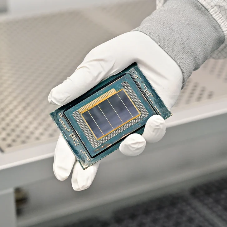
Intel's vice president and general manager for manufacturing development and customer engagement, Chris Auth, believes that his firm is better suited to using High NA EUV lithography machines than TSMC. Auth made the remarks during the Dwarkesh podcast, where he explained that since Intel relies on backside power delivery on its products, it can print circuits directly with High NA EUV.
The podcast also features the firm's chief technology officer (CTO) Pushkar Ranade, who explained that catching up with TSMC was a matter of scale and not technology.
RELATED STORY Intel’s Long-Delayed US Fab Expansion Gains Momentum As AI Demand Surges, Arizona Fab 62 Targets 2028 While Ohio One Hits Major Construction Milestone
Intel VP Says Backside Power Delivery Enables Firm To Use High NA EUV Machines
Since High NA EUV lithography machines increase the light's resolution on a wafer to enable a pitch ranging between 16-nanometer and 8-nanometer, it enables chip manufacturers to save costs by requiring a single pass. In lithography, a pitch is the space between two features, and manufacturers, such as TSMC, often print features in stages since a single stage does not have to adhere to tighter pitches as would have been the case if the design was printed in a single stage.
Speaking at the Dwarkesh podcast, Intel's Chris Auth commented that his firm will be able to rely on High NA since its pitch requirements are not as tight as TSMC's. This enables relaxed error tolerance, as looser pitches lower the need for precision when it comes to printing circuits.
According to him:
"We use backside power that means that you actually alleviate some of the pitch requirements you have on the front side. And that allows you to print that directly with High NA. TSMC has to run very tighter pitches because they don't have backside power and they can't do that with High NA so they have to use double patterning EUV."
Auth added that 14A is "an option in the PDK today and we're handling it as a customer by customer discussion."
The podcast also features the firm's chief technology officer (CTO) Pushkar Ranade, who explained that catching up with TSMC was a matter of scale and not technology.
RELATED STORY Intel’s Long-Delayed US Fab Expansion Gains Momentum As AI Demand Surges, Arizona Fab 62 Targets 2028 While Ohio One Hits Major Construction Milestone
Intel VP Says Backside Power Delivery Enables Firm To Use High NA EUV Machines
Since High NA EUV lithography machines increase the light's resolution on a wafer to enable a pitch ranging between 16-nanometer and 8-nanometer, it enables chip manufacturers to save costs by requiring a single pass. In lithography, a pitch is the space between two features, and manufacturers, such as TSMC, often print features in stages since a single stage does not have to adhere to tighter pitches as would have been the case if the design was printed in a single stage.
Speaking at the Dwarkesh podcast, Intel's Chris Auth commented that his firm will be able to rely on High NA since its pitch requirements are not as tight as TSMC's. This enables relaxed error tolerance, as looser pitches lower the need for precision when it comes to printing circuits.
According to him:
"We use backside power that means that you actually alleviate some of the pitch requirements you have on the front side. And that allows you to print that directly with High NA. TSMC has to run very tighter pitches because they don't have backside power and they can't do that with High NA so they have to use double patterning EUV."
Auth added that 14A is "an option in the PDK today and we're handling it as a customer by customer discussion."

Image Courtesy: Intel Corporation
Through backside power delivery, Intel transfers the power delivery circuitry on a chip to the backside of the silicon wafer. This frees up space for circuits at the 'front' of the wafer, where the computing transistors and the circuits that transfer data between them are located. Auth's comments confirm that the firm is now focused on the 14A process with the technology, while some earlier reports had discussed its use on the 18A node.
Continuing with TSMC, Intel's CTO, Pushkar Ranade, also discussed his firm's efforts to compete with the Taiwanese firm when it came to the global contract chip fabrication industry. Ranade admitted that TSMC is "a much larger wafer manufacturer today than we are" and added that "catching up in scale will be a slow process. And a gradual process."
However, he added that when it came to catching up in technology, Intel was "already there." While Intel "might maybe a few percent off on performance or power or area density but, you know, this sort of benchmarking of you know somewhat one foundry's ahead, or one foundry's behind" makes sense when one firm is a "whole generation" behind.
Stressing that execution is the key difference between Intel and TSMC, Ranade said:
"So you know you can be off by a few percent but you need to be on time. Your execution needs to be such that your yields are very high to support very large and very rapid ramps. So that actually is more important than catching up on a few percent on performance or area."
While Intel has repeatedly expressed optimism about its 14A manufacturing process technology, supply chain reports have also indicated that TSMC is accelerating its production timeline to lend weight to Ranade's claim.
Through backside power delivery, Intel transfers the power delivery circuitry on a chip to the backside of the silicon wafer. This frees up space for circuits at the 'front' of the wafer, where the computing transistors and the circuits that transfer data between them are located. Auth's comments confirm that the firm is now focused on the 14A process with the technology, while some earlier reports had discussed its use on the 18A node.
Continuing with TSMC, Intel's CTO, Pushkar Ranade, also discussed his firm's efforts to compete with the Taiwanese firm when it came to the global contract chip fabrication industry. Ranade admitted that TSMC is "a much larger wafer manufacturer today than we are" and added that "catching up in scale will be a slow process. And a gradual process."
However, he added that when it came to catching up in technology, Intel was "already there." While Intel "might maybe a few percent off on performance or power or area density but, you know, this sort of benchmarking of you know somewhat one foundry's ahead, or one foundry's behind" makes sense when one firm is a "whole generation" behind.
Stressing that execution is the key difference between Intel and TSMC, Ranade said:
"So you know you can be off by a few percent but you need to be on time. Your execution needs to be such that your yields are very high to support very large and very rapid ramps. So that actually is more important than catching up on a few percent on performance or area."
While Intel has repeatedly expressed optimism about its 14A manufacturing process technology, supply chain reports have also indicated that TSMC is accelerating its production timeline to lend weight to Ranade's claim.

One major recent development in the semiconductor industry has been the stacking of n-type and p-type transistors. These two transistors are the backbone of modern day manufacturing, and IBM recently announced the stacking approach as part of its plans for the 0.7-nanometer process node.
Intel's Jack Kavalieros, VP Components Research and a Fellow at the firm, discussed the problems in this approach. According to him:
"What used to be connections on the top or even of the bottom as you've seen from our press release, now has to go vertically in between the transistors. And that's a new challenge. Because the aspect ratio of creating trenches and filling those trenches becomes more and more difficult. So it's not as straightforward as stacking the transistors because you still have to think about interconnecting them."
The problem with the filling can leave air gaps and holes, he added.
Intel's Jack Kavalieros, VP Components Research and a Fellow at the firm, discussed the problems in this approach. According to him:
"What used to be connections on the top or even of the bottom as you've seen from our press release, now has to go vertically in between the transistors. And that's a new challenge. Because the aspect ratio of creating trenches and filling those trenches becomes more and more difficult. So it's not as straightforward as stacking the transistors because you still have to think about interconnecting them."
The problem with the filling can leave air gaps and holes, he added.

 Return to Top